The project
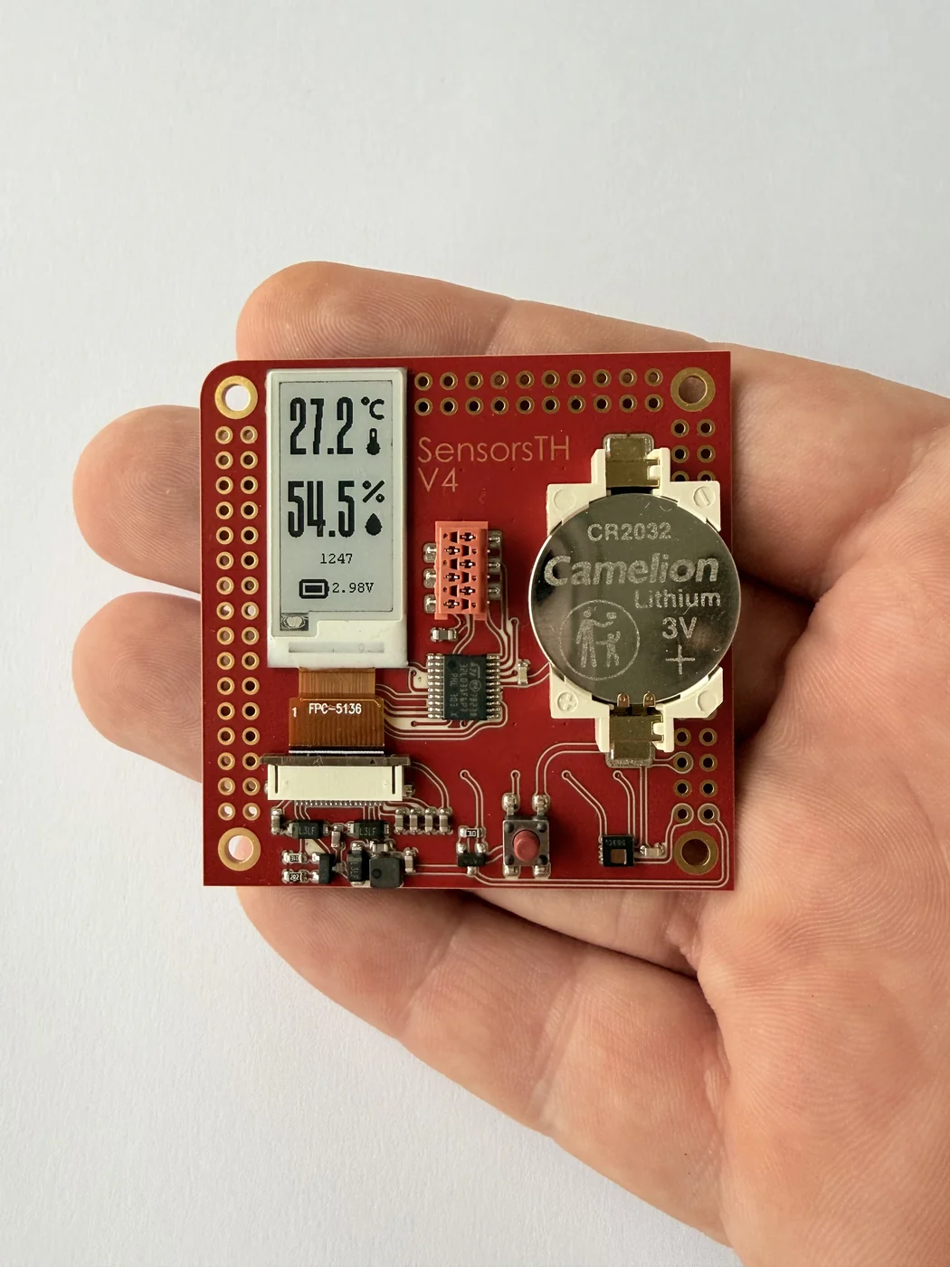
A small, working sensor board brings together a microcontroller, display connector, passives, and a battery holder. It gives us a concrete way to show the complete fabrication and assembly process.
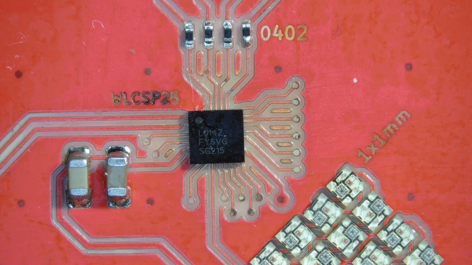
The board uses an STM32 in a TSSOP-20 package with a 0.65 mm pin pitch, an e-ink FPC connector with a 0.50 mm contact pitch, and 0603 passives.
A measured workflow
Start with prepared Gerber files and components ready to place. The benchmark covers fabrication and assembly through flashing the firmware; it does not include circuit design, layout, or writing the firmware.
- ≈10 min
PCB processing
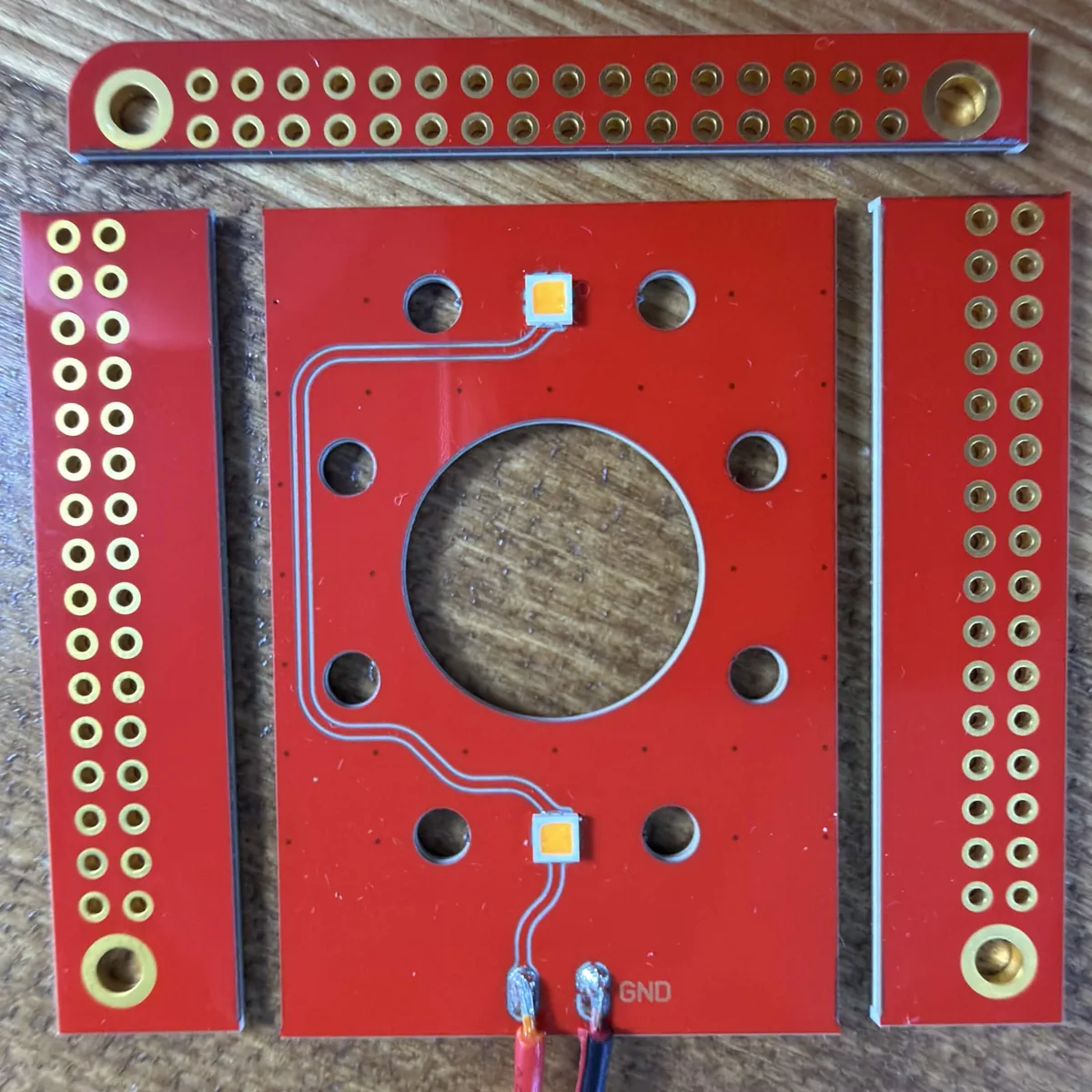
The laser processes the ceramic blank to form the board features.
- ≈5 min
Stencil and solder paste
Cut a tin stencil in place, apply solder paste, then peel off the stencil.
- ≈10 min
Component placement
Place the components by hand using tweezers.
- ≈5 min
Reflow soldering
Reflow the board on a small hot plate, then flash the firmware and check operation.
From the tray to working hardware
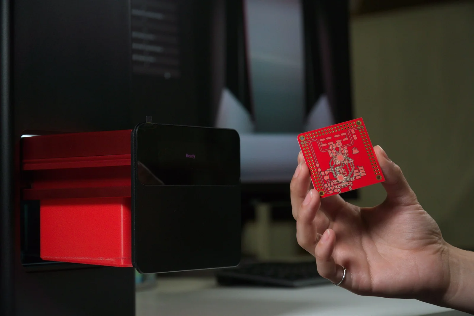
A short process video. The reported benchmark is specific to the Mini Weather Station.
What it demonstrates
Fine-pitch connectors and a working embedded system can be prototyped with a desktop fabrication workflow and manual assembly. The useful outcome is a board that can be powered, programmed, and tested.
For an engineering team, this makes it practical to evaluate a subsystem before committing it to the next product revision.