The challenge
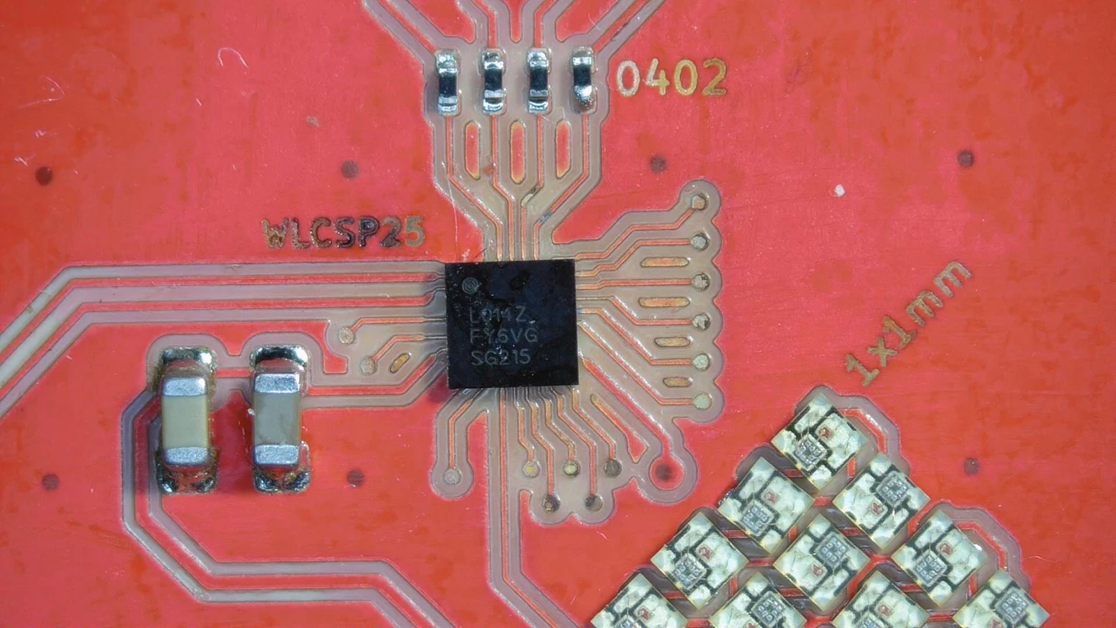
Fan out a tiny BGA on a single layer, then assemble the board by hand. The traces between the BGA pads are 50 µm wide, with clearances of about 70 µm in the tightest areas.
Prepare the board for assembly
The copper and solder-mask features are processed on PewCB One. For this fine-pitch layout, solder-mask restoration is a required extra step: it helps keep solder on the intended pads during reflow.
A single-use tin stencil is cut directly over the finished board. The apertures are aligned in place, and tin is deposited on the exposed pads during cutting. Apply solder paste, peel off the stencil, place the components, and reflow on a hot plate.
Small parts, deliberate preparation
The LEDs are SK6805-EC10 addressable parts measuring 1 × 1 mm. The resistors are 0201; the 0402 marking visible on the board is incorrect.
There is no pick-and-place machine in this demonstration. Components are placed by hand, with solder surface tension helping them settle on the pads during reflow.
What it demonstrates
The experiment shows a working route to fine-pitch hand assembly on a ceramic prototype. Success depends on the geometry, paste deposition, solder-mask preparation, and careful placement.